Combinational Circuit 1
Wadhwani Electronics Lab, IIT Bombay
Tuesday 10th August, 2021
Use structural modelling for this experiment; means instantiate components and use port map to connect those components
Part-A: 2x1 Mux
(i) VHDL description [5 Marks]
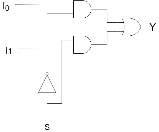
Write the VHDL description of a 2x1 multiplexer as shown in figure below.
info
Multiplexer is a combinational circuit that has maximum of data inputs, ‘n’ selection lines and single output line.
(ii) Write Truth table and boolean expression for output Y [3 Marks]
(iii) Simulation [5 Marks]
Simulate the 2x1 multiplexer using the generic testbench to confirm the correctness of your description.
note
To do this, use the tracefile given below and modify the testbench given to you appropriately.
Tracefile format
{<In1><In0><S> <Y> 1} Tracefile 📃
Part-B: 4x1 Mux
(i) Design [3 Marks]
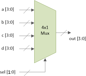
Design 4x1 Mux using only 2x1 Mux
info
data inputs
2 select lines
1 output line
(ii) VHDL description [5 Marks]
Write the VHDL description of a 4x1 multiplexer designed using 2x1 Mux.
(iii) Simulation [5 Marks]
Simulate the 4x1 multiplexer using the generic testbench to confirm the correctness of your description.
note
To do this, use the given tracefile and modify the testbench given to you appropriately.
Tracefile format<In4><In3><In2><In1><S2><S1> <Y> 1Tracefile 📃
Part-C: 4-bit 4x1 Mux
(i) Design [3 Marks]
Design 4-bit wide 4x1 Mux using only 4x1 Mux designed in part B.
(ii) VHDL description [5 Marks]
Write the VHDL description of a 4-bit wide 4x1 multiplexer designed using 4x1 Mux.
(iii) Simulation [5 Marks]
Simulate the 4-bit 4x1 multiplexer using the generic testbench to confirm the correctness of your description.
note
To do this, use the tracefile given below and modify the testbench given to you appropriately.
Tracefile format<d3 d2 d1 d0><c3 c2 c1 c0><b3 b2 b1 b0><a3 a2 a1 a0><sel1 sel0> <Y3Y2Y1Y0> 1111Tracefile 📃